
Beyond the Silicon Cage
Why Burson Builds Discrete Op-Amps
Intro
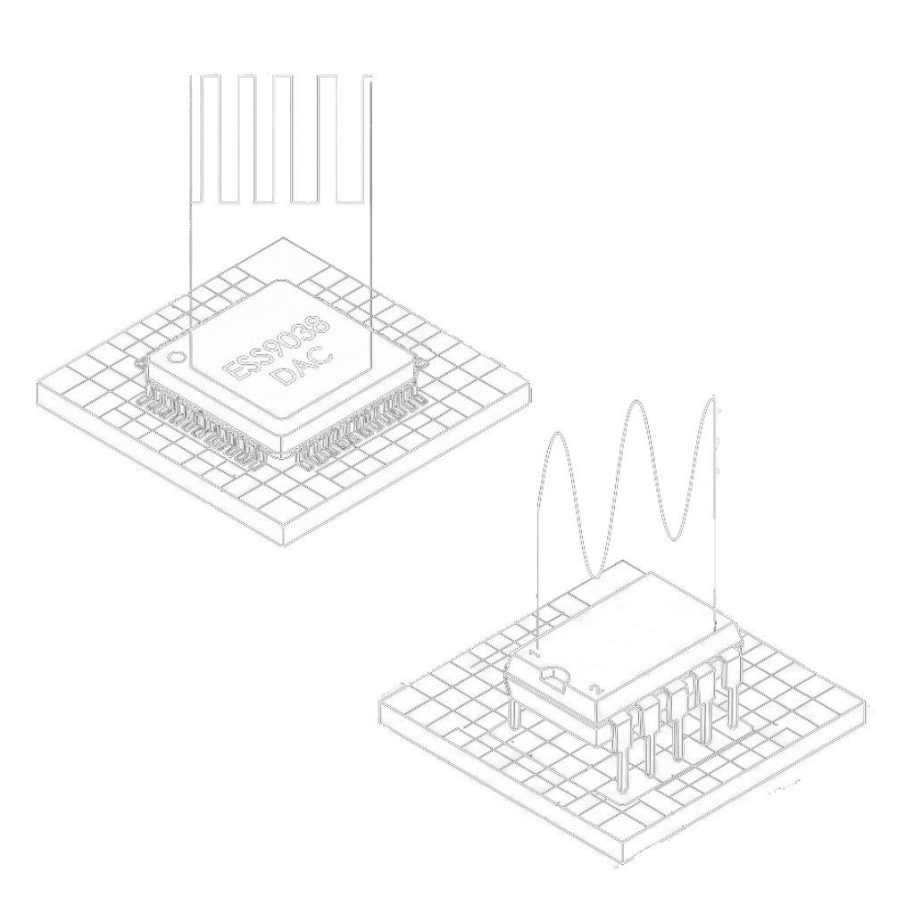
Integrated circuits (ICs) are the undisputed rulers of modern digital audio. They power your DAC chips, streamers, computers, and digital volume controllers with flawless execution. In the digital domain, where life is strictly parsed into ones and zeros, IC technology is an engineering marvel: it made electronics smaller, faster, cheaper, and profoundly reliable. Without them, modern digital audio simply wouldn’t exist.
But things get incredibly complicated the exact millisecond the music leaves the digital domain and becomes a living, breathing analogue waveform.
Once a DAC chip converts data into a continuously changing electrical voltage, the rules of the game change entirely. In the analogue domain, a circuit is no longer just recognizing a binary “on” or “off”. It is now tasked with protecting every micro-dynamic detail, delicate timing cue, and complex harmonic structure. This physical transition is where the strict limitations of silicon fabrication create a massive bottleneck—and it is precisely why Burson builds discrete op-amps.
Just Like Your Camera Lens
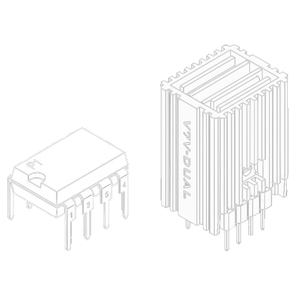
The operational amplifier, or op-amp, is the foundational building block of modern audio design. Found everywhere from preamps and headphone amplifiers to critical DAC output stages, op-amps handle vital tasks like voltage gain, filtering, and impedance matching. They are the hidden engines driving your entire system’s analogue performance.
Right after digital-to-analogue conversion, the op-amp handles the most high-stress analogue stages: current-to-voltage (I/V) conversion and low-pass filtering. Think of these early analogue stages like a high-end camera lens:
A camera sensor can possess a world-class, ultra-high resolution, but if the lens in front of it is optically warped, every single image captured through it will be permanently compromised.
The same rule applies to audio. The music signal coming directly out of a modern DAC chip is full of ultra-fast current pulses and high-frequency digital switching noise. Any tiny distortion, timing error, or loss of detail introduced at this foundational op-amp stage will be permanently baked into the waveform and amplified by every component that follows.
High-fidelity audio plays by unforgiving rules. If an analogue gain stage is asked to multiply a signal by exactly ten, the output must be a pristine 10.00—not 9.99 or 10.01. Any microscopic deviation physically warps the shape of the waveform, which is the literal definition of distortion.
The Transistor Problem: "Fingering" and Hidden Parasitics
To achieve flawless waveform accuracy, differential audio circuits demand absolute component matching and symmetry. However, creating identical microscopic transistors on a single silicon die is virtually impossible due to natural manufacturing variations across a silicon wafer.
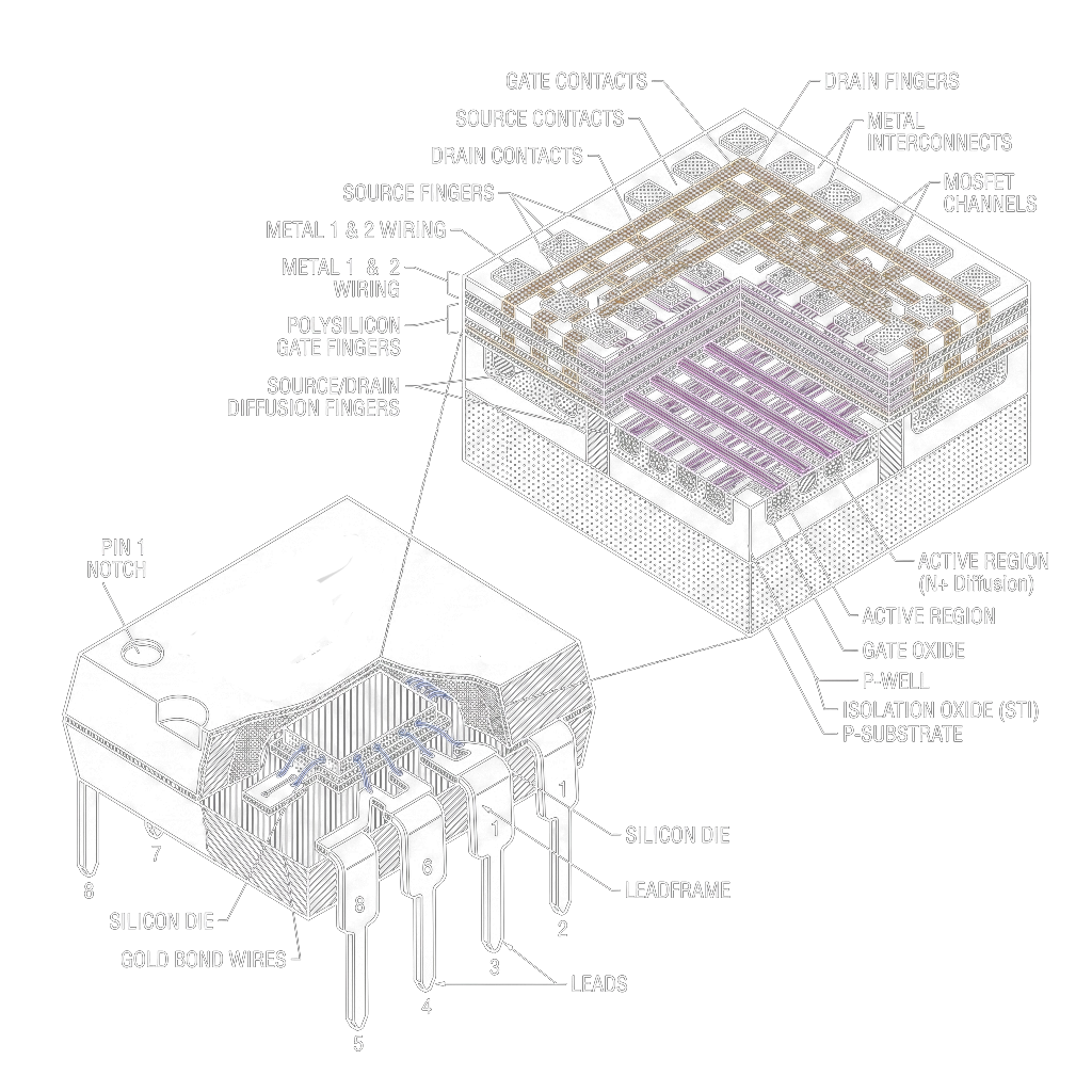
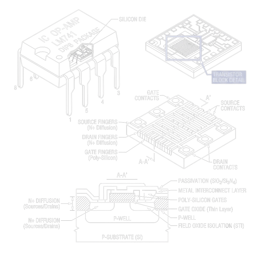
Inside an IC op-amp, designers cannot pull individual transistors off the line to hand-test and match them. Instead, they rely on a geometric layout workaround called Fingering.
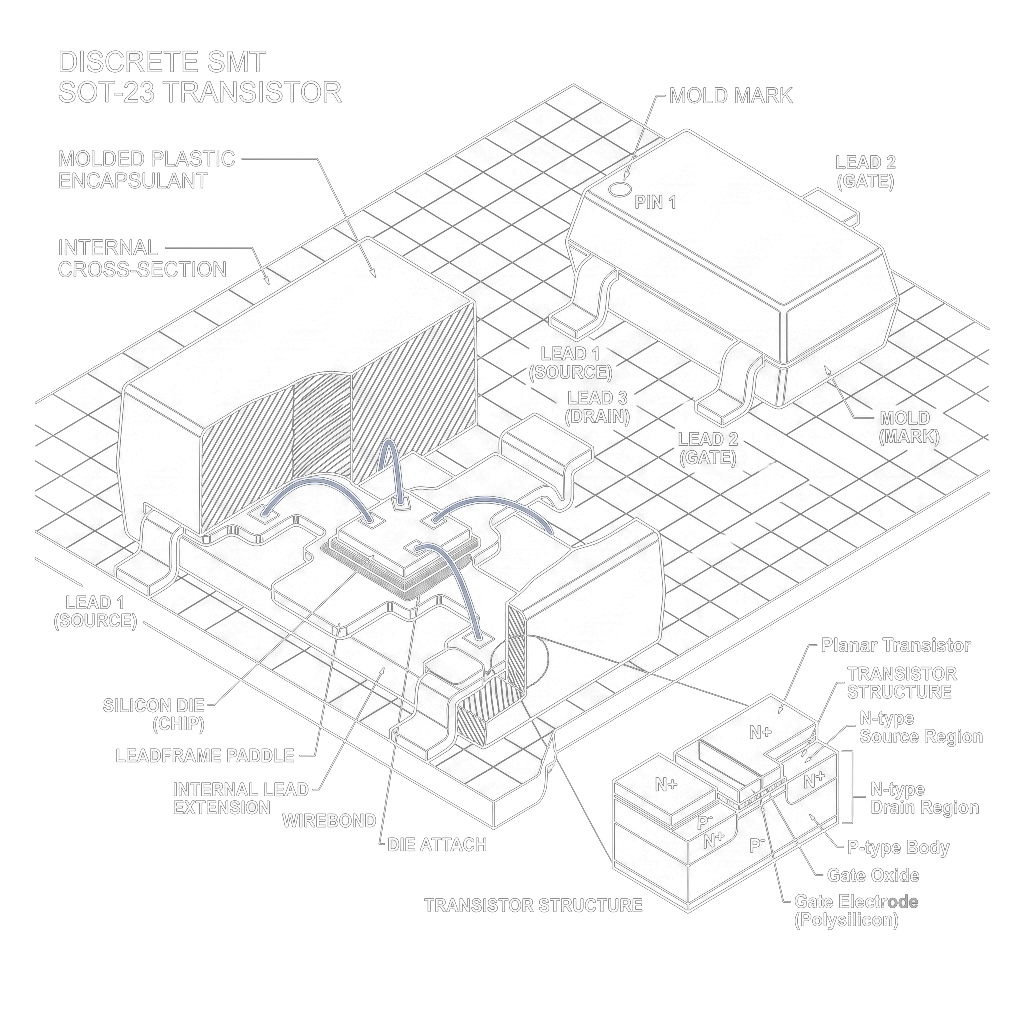
Rather than implementing one large, unified transistor, the device is chopped up into multiple smaller parallel segments called “fingers” spread across a section of the silicon to average out manufacturing errors.
While fingering serves as a clever statistical patch for mass production, it introduces a severe structural compromise for high-end analogue audio. Once a transistor is divided into a fragmented structure, it no longer behaves as a single, coherent device. Each individual finger features its own distinct physical routing, resistance, and—crucially—stray parasitic capacitance.
Instead of an instantaneous, unified response, this layout creates a distributed RC effect. In the gigahertz realm of RF design, this causes timing delays; in high-fidelity audio, these parasitic high-frequency phase non-linearities pollute the circuit. When the active device responds through a fragmented structure, fast musical transients—like the sharp leading edge of a snare drum or the crisp pluck of an acoustic guitar string—become slightly softened, blurred, or smeared.
Burson avoids this geometric compromise entirely. By using discrete, individually selected transistors, we have the freedom to hand-test and perfectly match individual transistor pairs on the test bench before they ever meet the PCB. One transistor means one unified device, preserving a clean, lightning-fast, and completely direct transient response.
The Asymmetry Trap: The Legacy IC Bottleneck
High-fidelity push-pull audio circuits require an absolute, mirror-image symmetry between NPN transistors (which process the positive half of the audio wave) and PNP transistors (which process the negative half).
Semiconductor physics, however, makes this a steep hill to climb: electrons (NPN) naturally move three times faster than holes (PNP), meaning raw PNP devices are inherently sluggish by nature. In the discrete manufacturing world, we can equalize these speeds using advanced chemical treatments like Strained Silicon-Germanium (SiGe) Epitaxy to compress the crystal lattice and boost hole mobility, alongside heavy-metal treatments to sharpen turn-off times.
Inside a shared silicon wafer, this level of independent optimization is an uphill battle. While a handful of ultra-advanced, modern ICs deploy specialized complementary processes to mitigate this, the absolute reality of the audio market is that the vast majority of audio equipment still relies on ubiquitous, deeply entrenched legacy ICs (like the legendary NE5532 and NE5534).
These standard, mass-market ICs bypass the manufacturing roadblock by optimizing exclusively for the fast NPN transistor, leaving the negative audio signal to rely on a severely compromised Lateral PNP layout. This configuration forces the negative half of the current to travel sideways across leftover surface layers of the die, resulting in a sluggish, noisy, and inherently asymmetric gain stage.
Burson eliminates this shared substrate trap entirely. By utilizing independently manufactured vertical NPN and PNP transistors—each structurally and chemically optimized on its own dedicated wafer line—we achieve uncompromised, true mirror-image audio symmetry.
The Resistor Problem: Interdigitation vs. Absolute Precision
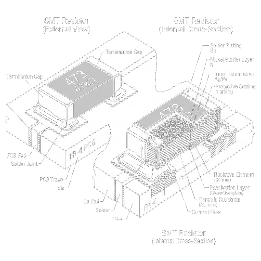
Resistors face an identical hurdle inside silicon fabrication. When Burson selects a physical precision resistor, its value is factory-certified down to a strict 0.1% tolerance before it enters the circuit.
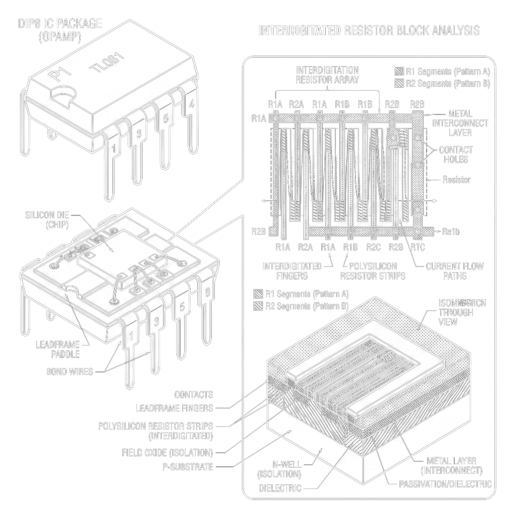
Inside an IC, guaranteeing absolute resistor values is incredibly difficult. To work around this, IC layout relies on a geometric technique called Interdigitation—dividing resistors into small segments and physically weaving them together like interlocking fingers.
This ensures that if the underlying material properties shift during manufacturing, the ratio between the resistors stays relatively stable, even if their absolute standalone values are completely off target.
Interdigitation is not an audio performance feature; it is a manufacturing workaround because the silicon fabrication process cannot naturally provide the absolute precision that high-end analogue circuits demand. Weaving these microscopic traces together creates a maze of geometric complexity, injecting unwanted stray parasitic capacitances directly into the critical signal path.
The Ultimate Bottleneck: Thermal Coupling & The Feedback Trap
What happens when an IC die suffers from these native layout non-linearities, minor transistor mismatches, and geometric parasitics? To make the numbers look perfect on a datasheet, IC designers are forced to use massive open-loop gain and apply aggressive, deep global negative feedback. This high-feedback trap is precisely what gives many standard IC designs their notoriously sterile, flat, and dynamically constricted sonic signature.
Compounding this issue is an insurmountable physical limitation: Thermal Coupling.
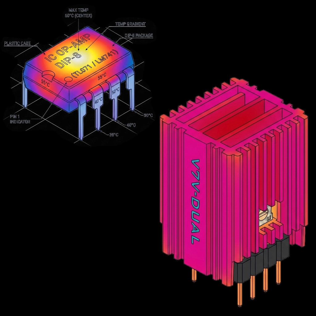
Because all internal transistors share the exact same tiny silicon substrate, they suffer from intense thermal crosstalk. When the output stage of the IC handles a demanding audio signal and generates heat, that thermal energy instantly flashes across the tiny die, warping the behavior of the sensitive, ultra-low-signal input stages sitting just micrometers away. Because transistor behavior changes drastically with temperature, this thermal coupling causes internal matching to constantly drift and linearity to suffer under dynamic musical loads.
This thermal cage creates a hard physical ceiling: an IC op-amp can never run in Pure Class-A.
True, high-bias Class-A operation requires a heavy, continuous standing current, which generates significant, constant heat. If you biased a microscopic IC aggressively enough to achieve true Class-A, the internal thermal coupling would instantly destabilize the circuit, cause thermal runaway, and literally destroy the chip. Consequently, IC op-amps are forced to run in highly efficient, lower-bias modes.
The Burson V7 Pro is engineered with total thermal freedom. Its discrete components are physically separated, entirely preventing thermal crosstalk. More importantly, its precision-machined aluminum enclosure acts as a high-capacity external heatsink, safely and continuously dissipating the heat generated by true, uncompromised, high-bias Class-A operation. Natively linear from the start, it requires minimal, highly optimized feedback—preserving natural acoustic space, rich macro-dynamics, and pure decay cues.
Dismantling the "Shrunk-Down" Myth
The integrated op-amp is undoubtedly one of the most successful cost-saving and space-saving inventions in human history. However, because mass-market manufacturers routinely gloss over the severe fabrication shortcuts required to make these chips work, a common consumer misconception has formed.
Many music lovers believe that an IC op-amp is simply a perfect, microscopic “shrunken-down version” of a discrete circuit.
As the physics demonstrates, it is not. An IC op-amp is a fundamentally different architecture defined by compromises like fingering layout patches, interdigitation parasitics, lateral signal paths, and severe thermal restrictions.
By moving beyond the silicon cage, Burson eliminates these workarounds. We use real precision components, real physical separation, and authentic Class-A operating conditions. We build discrete op-amps because performance should always take absolute priority over manufacturing convenience the second a signal becomes music.
Published References
For the final Burson article, I would use these as the strongest and cleanest references:
- Texas A&M ECEN 474 — Lecture 6: Layout Techniques
https://people.engr.tamu.edu/spalermo/ecen474/lecture06_ee474_layout.pdf - Texas A&M ECEN 474/704 — Lab 2: Layout Design
https://people.engr.tamu.edu/spalermo/ecen474/Lab2.pdf - UC Berkeley EECS 240 — CMOS Passive Devices Lecture
https://rfic.eecs.berkeley.edu/courses/ee240sp06/pdf/lect2.pdf - P. E. Allen — CMOS Analog Circuit Design, Lecture 7: Resistors and Inductors
https://aicdesign.org/wp-content/uploads/2018/08/lecture07-140310.pdf - P. E. Allen — CMOS Analog Circuit Design, Lecture 12: Component Matching
https://aicdesign.org/wp-content/uploads/2018/08/lecture12-140610.pdf - IIT Madras — Analog Layout Techniques
https://www.ee.iitm.ac.in/vlsi/_media/courses/ee5325_2019/ee5325_lecture48_6nov2019.pdf - IEEE JSSC — Analog Layout Using ALAS!
https://cmosedu.com/jbaker/papers/1996/JSSC311996.pdf - Chalmers University — Substrate Noise Coupling in Mixed-Signal Integrated Circuits
https://research.chalmers.se/publication/48130/file/48130_Fulltext.pdf - Texas Instruments — Understanding Operational Amplifier Specifications
https://www.ti.com/lit/pdf/sloa011 - Microelectronics Reliability — Impact of Multi-Finger MOSFET Geometry
https://hal.science/hal-03604352v1/file/Microelectronics_Reliability_2022_-SS_FH_VF.pdf